8位MCU-MC9S08LG32的LCD驱动设计方案
本文介绍了MC9S08LG32系列的主要特性,方框图,以及演示板DEMO9S08LG32的主要特性和电路图。Freescale 公司的MC9S08LG32系列包括MC9S08LG32 和MC9S08LG16,采用8位HCS08 CPU,2.7V-5.5V时CPU高达40MHz,工作温度为-40℃到85℃和-40℃到105℃两种.支持多达32种中断/重置源,具有多种外设如LCD,ADC,以及SCI,SPI,I2C,TPMx,MtiM,RTC,KBI和IRQ,主要应用在工业HVAC系统,电表,家用电器,医疗设备,仪表,无线传感器应用,安防系统和个人保健设备。
The MC9S08LG family of 8-bit microcontrollers drives liquid crystal displays (LCD) with up to 296 segments. This 5V LCD device offers improved performance and flexible pin functionality for a wide range of industrial and automotive applications, such as electric metering, home appliances, HVAC systems and entry level instrument clusters.
MC9S08LG32 Series Covers: MC9S08LG32 and MC9S08LG16
MC9S08LG32主要特性:
8-bit HCS08 Central Processor Unit (CPU)
Up to 40 MHz CPU at 5.5 V to 2.7 V across temperature range of –40℃ to 85℃ and -40℃ to 105℃
HCS08 instruction set with added BGND instruction
Support for up to 32 interrupt/reset sources
On-Chip Memory
32 KB or 18 KB dual array flash; read/program/erase over full operating voltage and temperature
1984 byte random access memory (RAM)
Security circuitry to prevent unauthorized access to RAM and flash contents
Power-Saving Modes
Two low-power stop modes (stop2 and stop3)
Reduced-power wait mode
Peripheral clock gating register can disable clocks to unused modules, thereby reducing currents
Low power on-chip crystal oscillator (XOSC) that can be used in low-power modes to provide accurate clock source to real time counter and LCD controller
100 μs typical wakeup time from stop3 mode
Clock Source Options
Oscillator (XOSC) — Loop-control Pierce oscillator; crystal or ceramic resonator range of 31.25 kHz to 38.4 kHz or 1 MHz to 16 MHz
Internal Clock Source (ICS) — Internal clock source module containing a frequency-locked-loop (FLL) controlled by internal or external reference; precision trimming of internal reference allows 0.2% resolution and 2% deviation over temperature and voltage; supports bus frequencies from 1 MHz to 20 MHz.
System Protection
COP reset with option to run from dedicated 1 kHz internal clock or bus clock
Low-voltage warning with interrupt
Low-voltage detection with reset
Illegal opcode detection with reset
Illegal address detection with reset
Flash and RAM protection
Development Support
Single-wire background debug interface
Breakpoint capability to allow single breakpoint setting during in-circuit debugging (plus two more breakpoints in on-chip debug module)
On-chip in-circuit emulator (ICE) debug module containing three comparators and nine trigger modes; eight deep FIFO for storing change-of-flow addresses and event-only data;debug module supports both tag and force breakpoints
Peripherals
LCD — Up to 4 × 41 or 8 × 37 LCD driver with internal charge pump.
ADC — Up to 16-channel, 12-bit resolution; 2.5 μs conversion time; automatic compare function; temperature sensor; internal bandgap reference channel; runs in stop3 and can wake up the system; fully functional from 5.5 V to 2.7 V
SCI — Full duplex non-return to zero (NRZ); LIN master extended break generation; LIN slave extended break detection; wakeup on active edge
SPI — Full-duplex or single-wire bidirectional; double-buffered transmit and receive; master or slave mode; MSB-first or LSB-first shifting
IIC — With up to 100 kbps with maximum bus loading; multi-master operation;programmable slave address; interrupt driven byte-by-byte data transfer; supports broadcast mode and 10-bit addressing
TPMx — One 6 channel and one 2 channel; selectable input capture, output compare, or buffered edge or center-aligned PWM on each channel
MTIM — 8-bit counter with match register; four clock sources with prescaler dividers; can be used for periodic wakeup
RTC — 8-bit modulus counter with binary or decimal based prescaler; three clock sources including one external source; can be used for time base, calendar, or task scheduling functions
KBI — One keyboard control module capable of supporting 8 × 8 keyboard matrix
IRQ — External pin for wakeup from low-power modes
Input/Output
39, 53, or 69 GPIOs
8 KBI and 1 IRQ interrupt with selectable polarity
Hysteresis and configurable pullup device on all input pins; configurable slew rate and drive strength on all output pins.
Package Options
48-pin LQFP, 64-pin LQFP, and 80-pin LQFP
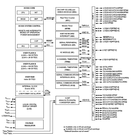
图1.MC9S08LG32系列方框图
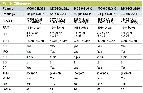
下表为MC9S08LG32系列器件的主要参数指标:
MC9S08LG32目标应用:
Industrial HVAC system
Electric metering
Home appliance
Medical application
Instrumentation
Personal care devices
Wireless sensor applications
Security systems
Automotive
MC9S08LG32演示板DEMO9S08LG32
The DEMO9S08LG32 is a demonstration board for the MC9S08LG32 8-bit microcontroller. Application development is quick and easy with the integrated USB-BDM, sample software tools and examples. An optional BDM_PORT port is also provided to allow use of a BDM_PORT cable. One, 80-pin connector provides access to all IO signals on the target MCU.
DEMO9S08LG32主要特性:
1.MC9S08LG32, 80 LQFP
2.On-board 4x40 custom LCD glass
3.Integrated P&E USB-BDM
4.On-board +5V regulator
5.10 push switches; 8 user, 1 reset, 1 IRQ
6.12 LED indicators; 8 user, VDD, IRQ, USB, and reset
7.5K ohm POT w /LP filter for ADC input
8.80-pin MCU I/O pin header
9.2.0mm barrel connector
10.USB connector
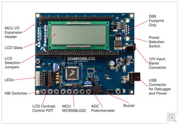
图2.DEMO9S08LG32演示板外形图
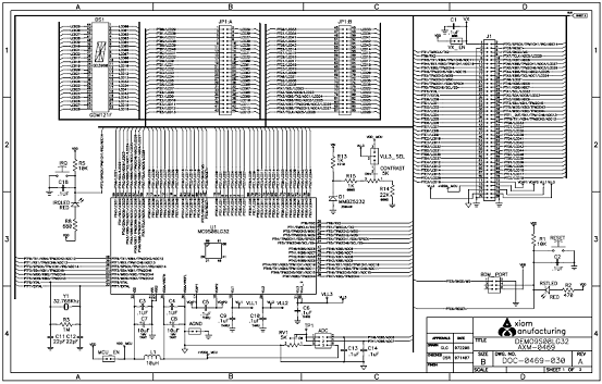
DEMO9S08LG32电路图
图3.DEMO9S08LG32电路图(1)
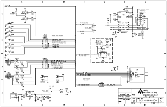
图4.DEMO9S08LG32电路图(2)
 0
0


 /9
/9 


 淘帖
淘帖 5665
5665

