对于您的问题,产品线工程师答复如下,供您参考。
This is not the first time cascaded AD8367 have been used to extend the dynamic range. There are a few things one must keep in mind while cascading the VGAs to extend the dynamic range:
1) The input linearity of the cascade will be very low at high gain settings
2) The sensitivity will be poor at low gain settings
3) High max gain and high bandwidth devices like the AD8367 may be potentially unstable, and it may be necessary to apply some resistive padding between the stages to ensure a stable solution.
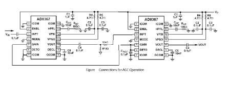
Starting with the third point, it will likely be necessary to add ~10dB of padding between the two VGA's (or all three VGAs if you need it, right now, I’ll just speak to two cascaded VGAs). The AD8367 needs to be sourced and loaded in a 200-Ohm impedance environment to ensure stability. However, the output of the AD8367 presents a 50-Ohm impedance. If you directly cascade the devices the 2nd stage VGA will be presented by the 50-Ohm impedance of the first stages output, and may cause the 2nd stage to oscillate. As a result a 200-Ohm to 200-Ohm resistive pad will likely be needed between the two stages. A 10dB pad should be enough to isolate the 50-Ohm source impedance of the first stage VGA from the input of the second stage. If the cascade is properly stabilized, you should be able to achieve ~90dB of gain adjustment range.
You will probably have to either LC matching or baluns/transformer on the input of the first VGA and the output of the second VGA to get the 50 Ohms to 200 Ohm match. This will help with the MDS and the Noise Figure of the system.
也建议您在级间增加pi衰网络。
对于您的问题,产品线工程师答复如下,供您参考。
This is not the first time cascaded AD8367 have been used to extend the dynamic range. There are a few things one must keep in mind while cascading the VGAs to extend the dynamic range:
1) The input linearity of the cascade will be very low at high gain settings
2) The sensitivity will be poor at low gain settings
3) High max gain and high bandwidth devices like the AD8367 may be potentially unstable, and it may be necessary to apply some resistive padding between the stages to ensure a stable solution.
Starting with the third point, it will likely be necessary to add ~10dB of padding between the two VGA's (or all three VGAs if you need it, right now, I’ll just speak to two cascaded VGAs). The AD8367 needs to be sourced and loaded in a 200-Ohm impedance environment to ensure stability. However, the output of the AD8367 presents a 50-Ohm impedance. If you directly cascade the devices the 2nd stage VGA will be presented by the 50-Ohm impedance of the first stages output, and may cause the 2nd stage to oscillate. As a result a 200-Ohm to 200-Ohm resistive pad will likely be needed between the two stages. A 10dB pad should be enough to isolate the 50-Ohm source impedance of the first stage VGA from the input of the second stage. If the cascade is properly stabilized, you should be able to achieve ~90dB of gain adjustment range.
You will probably have to either LC matching or baluns/transformer on the input of the first VGA and the output of the second VGA to get the 50 Ohms to 200 Ohm match. This will help with the MDS and the Noise Figure of the system.
也建议您在级间增加pi衰网络。

 举报
举报