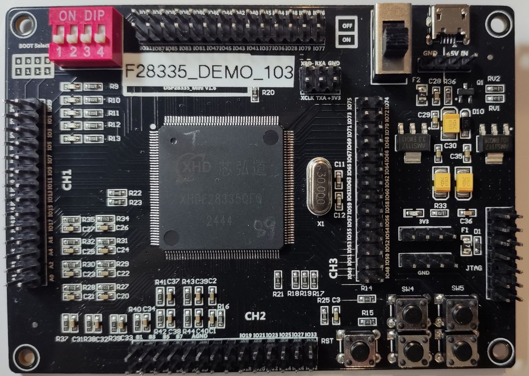
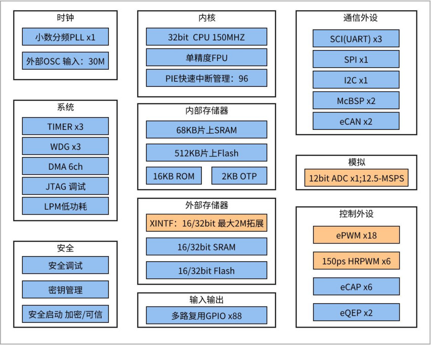
六岳微 LY-F335 开发板采用 32 位自主内核设计,主频 150MHz,集成了大量外设部件,具有高性能、低功耗和高可靠性的特点。应用于电机控制、光伏逆变、数字电源等领域。
动态展示见顶部视频。
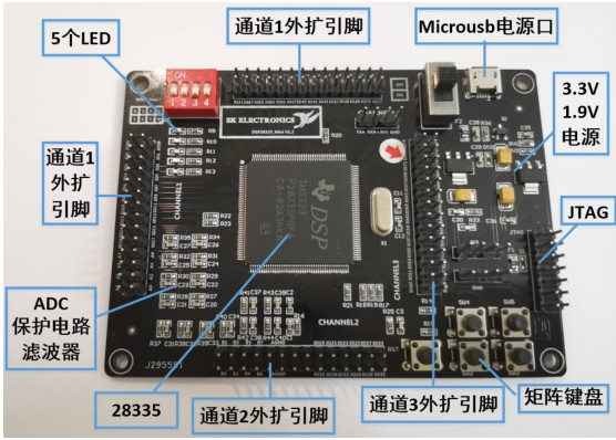
XHDF28335 是一款全自主正向设计的高性能浮点DSP芯片,采用32位自主内核设计,主频为150MHz,内部集成了丰富的外设资源,支持多种通信协议,具有 高性能、低功耗和高可靠性的特点。
广泛应用于变频器、电机控制、光伏逆变、数字电源等领域。
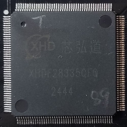
详见:芯弘道 | XHDF28335 .
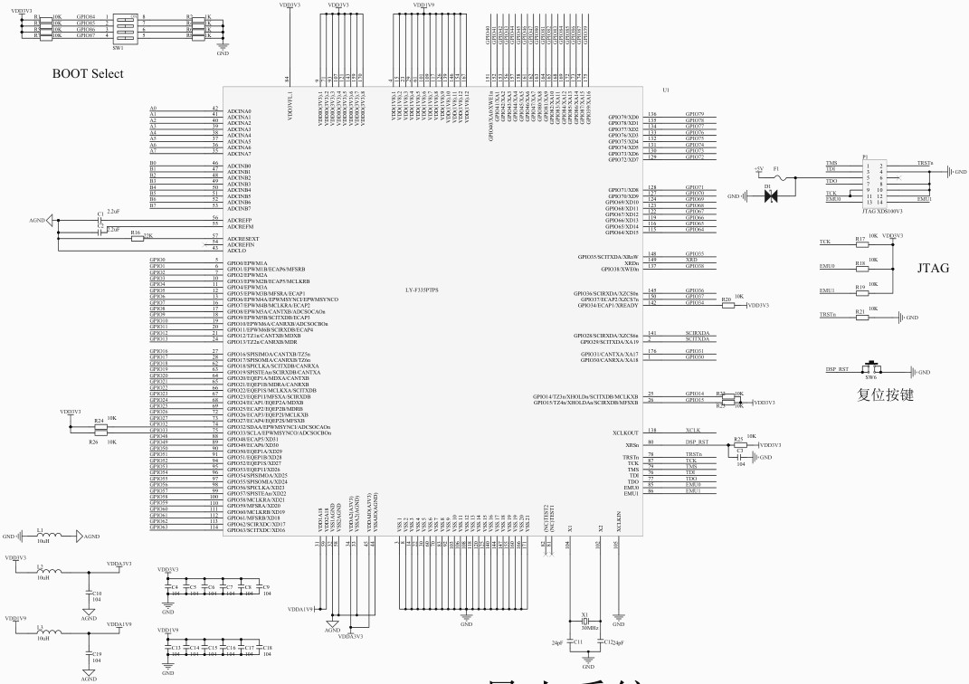
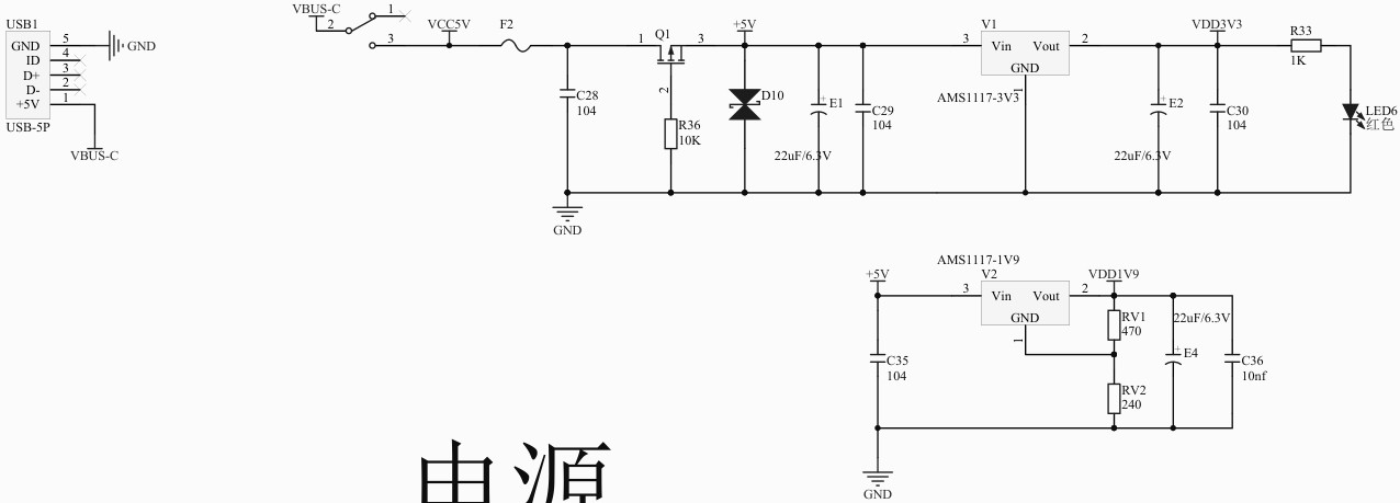
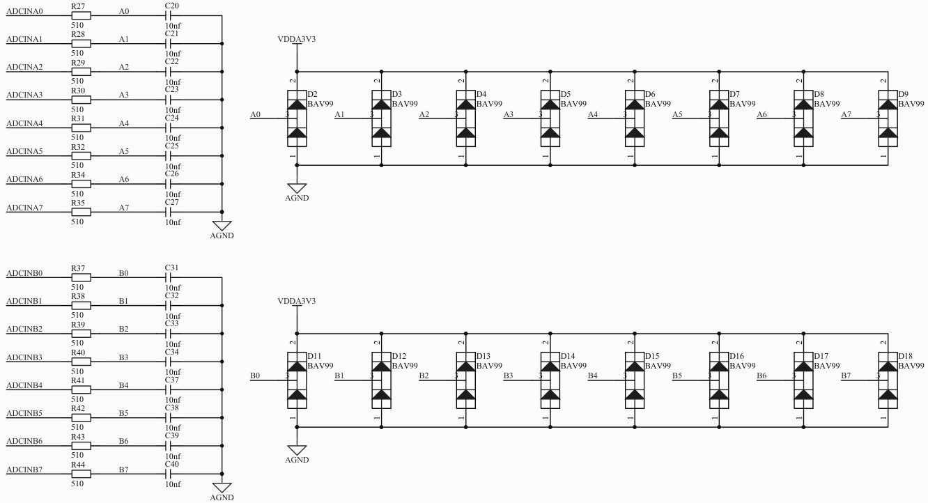
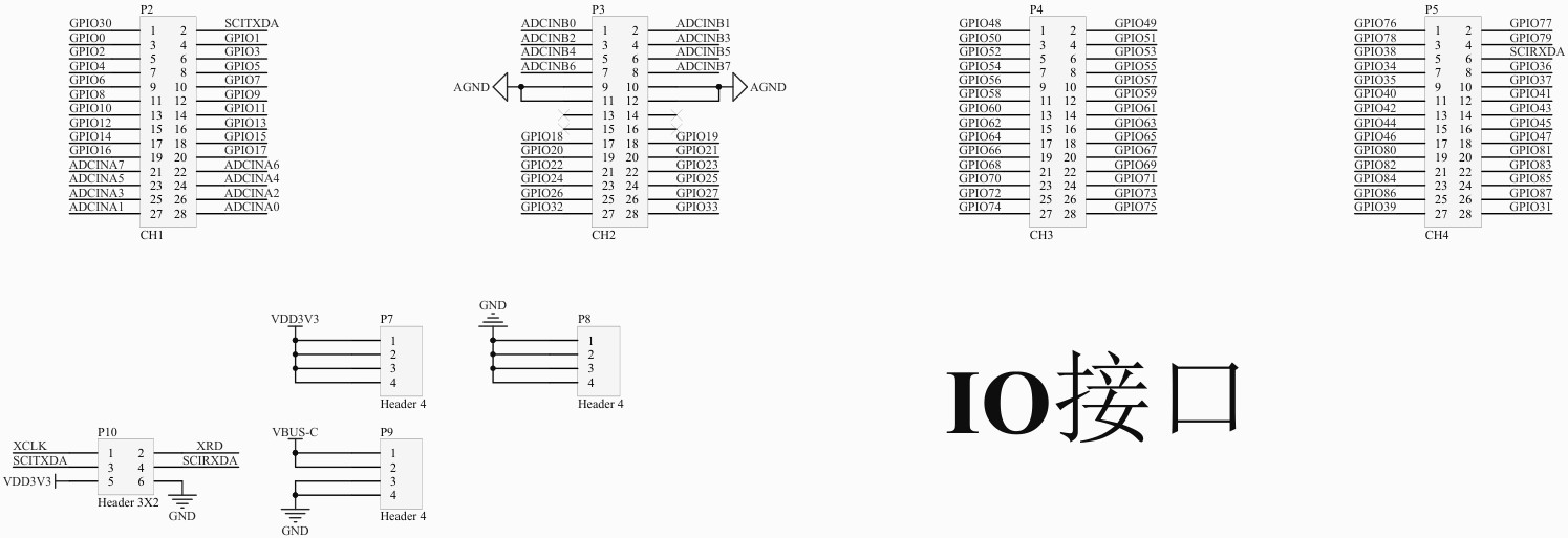
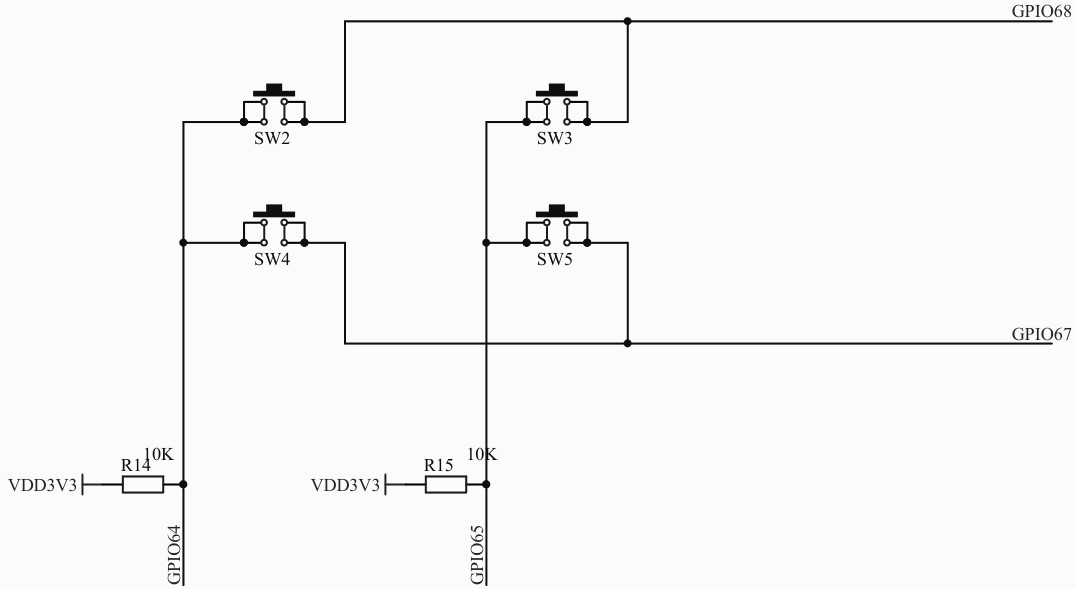
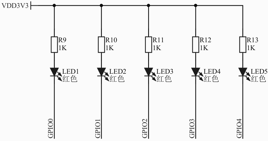
包括 MCU、供电、GPIO、外设、ADC等。
进入产品资料链接目录 LY-F335/软件开发资源 ,下载 SDK 压缩包;
下载 C2000Ware_3_04_00_00_setup.exe 并安装 C2000Ware 软件;
下载 ti_cgt_c2000_6.4.2_windows_installer.exe 并安装 C2000 Code Generation Tools;
下载并安装 CCSTUDIO IDE .
详细安装步骤见压缩包内教程。
File - Import Project ,选择 C2000 安装例程 F:\ti\c2000\C2000Ware_3_04_00_00\device_support\f2833x\examples\gpio_toggle 文件夹;
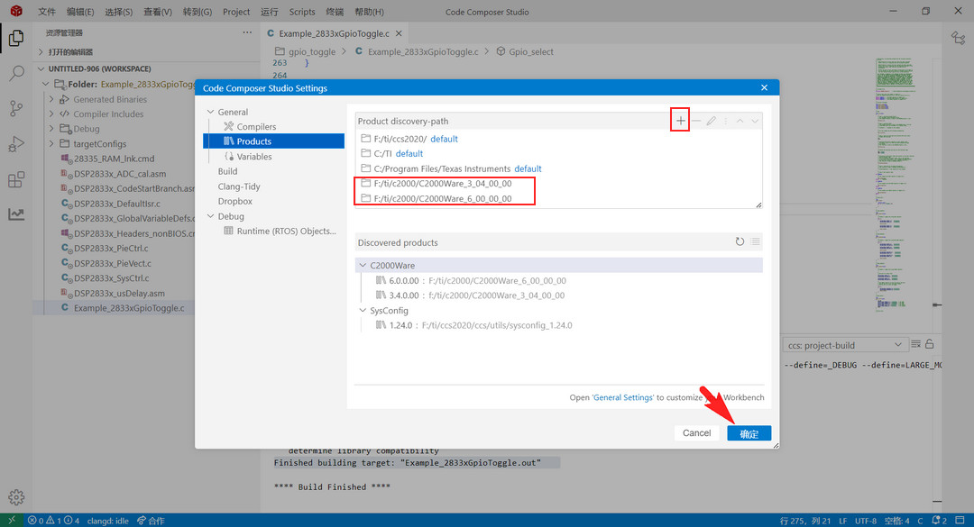
File - 首选项 - Code Composer Studio Settings - General - Products,添加 C2000Ware 安装文件夹路径;
右键工程 - Build Project
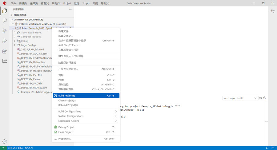
终端打印 构建完成,生成 *.out 文件
Finished building target: "Example_2833xGpioToggle.out"
双击打开左侧 Demo 目录文件 Example_2833xGpioToggle.c
#include "DSP28x_Project.h"     // Device Headerfile and Examples Include File

//
// Defines that select the example to compile in.
// Only one example should be set as 1 the rest should be set as 0.
//
#define EXAMPLE1 1  // Use DATA registers to toggle I/O's
#define EXAMPLE2 0  // Use SET/CLEAR registers to toggle I/O's
#define EXAMPLE3 0  // Use TOGGLE registers to toggle I/O's

//
// Function Prototypes
//
void delay_loop(void);
void Gpio_select(void);
void Gpio_example1(void);
void Gpio_example2(void);
void Gpio_example3(void);

//
// Main
//
void main(void)
{
    //
    // Step 1. Initialize System Control:
    // PLL, WatchDog, enable Peripheral Clocks
    // This example function is found in the DSP2833x_SysCtrl.c file.
    //
    InitSysCtrl();

    //
    // Step 2. Initialize GPIO:
    // This example function is found in the DSP2833x_Gpio.c file and
    // illustrates how to set the GPIO to it's default state.
    //
    // InitGpio();  // Skipped for this example

    //
    // For this example use the following configuration
    //
    Gpio_select();

    //
    // Step 3. Clear all interrupts and initialize PIE vector table
    // Disable CPU interrupts
    //
    DINT;

    //
    // Initialize PIE control registers to their default state.
    // The default state is all PIE interrupts disabled and flags
    // are cleared.
    // This function is found in the DSP2833x_PieCtrl.c file.
    //
    InitPieCtrl();

    //
    // Disable CPU interrupts and clear all CPU interrupt flags
    //
    IER = 0x0000;
    IFR = 0x0000;

    //
    // Initialize the PIE vector table with pointers to the shell Interrupt
    // Service Routines (ISR).
    // This will populate the entire table, even if the interrupt
    // is not used in this example.  This is useful for debug purposes.
    // The shell ISR routines are found in DSP2833x_DefaultIsr.c.
    // This function is found in DSP2833x_PieVect.c.
    //
    InitPieVectTable();

    //
    // Step 4. Initialize all the Device Peripherals:
    // This function is found in DSP2833x_InitPeripherals.c
    //
    // InitPeripherals(); // Not required for this example

    //
    // Step 5. User specific code:
    //
#if EXAMPLE1
    //
    // This example uses DATA registers to toggle I/O's
    //
    Gpio_example1();
#endif  // - EXAMPLE1

#if EXAMPLE2
    //
    // This example uses SET/CLEAR registers to toggle I/O's
    //
    Gpio_example2();
#endif

#if EXAMPLE3
    //
    // This example uses TOGGLE registers to toggle I/O's
    //
    Gpio_example3();
#endif
}

//
// delay_loop -
//
void
delay_loop()
{
    volatile long i;
    for (i = 0; i < 1000000; i++)
    {

    }
}

//
// Gpio_example1 -
//
void
Gpio_example1(void)
{
    //
    // Example 1: Toggle I/Os using DATA registers
    //
    for(;;)
    {
        GpioDataRegs.GPADAT.all    =0xAAAAAAAA;
        GpioDataRegs.GPBDAT.all    =0x0000000A;

        delay_loop();

        GpioDataRegs.GPADAT.all    =0x55555555;
        GpioDataRegs.GPBDAT.all    =0x00000005;

        delay_loop();
    }
}

//
// Gpio_example2 -
//
void
Gpio_example2(void)
{
    //
    // Example 2: Toggle I/Os using SET/CLEAR registers
    //
    for(;;)
    {
        GpioDataRegs.GPASET.all    =0xAAAAAAAA;
        GpioDataRegs.GPACLEAR.all  =0x55555555;

        GpioDataRegs.GPBSET.all    =0x0000000A;
        GpioDataRegs.GPBCLEAR.all  =0x00000005;

        delay_loop();

        GpioDataRegs.GPACLEAR.all    =0xAAAAAAAA;
        GpioDataRegs.GPASET.all      =0x55555555;

        GpioDataRegs.GPBCLEAR.all    =0x0000000A;
        GpioDataRegs.GPBSET.all      =0x00000005;

        delay_loop();
    }
}

//
// Gpio_example3 -
//
void
Gpio_example3(void)
{
    //
    // Example 2: Toggle I/Os using TOGGLE registers
    //

    //
    // Set pins to a known state
    //
    GpioDataRegs.GPASET.all    =0xAAAAAAAA;
    GpioDataRegs.GPACLEAR.all  =0x55555555;

    GpioDataRegs.GPBSET.all    =0x0000000A;
    GpioDataRegs.GPBCLEAR.all  =0x00000005;

    //
    // Use TOGGLE registers to flip the state of the pins.
    // Any bit set to a 1 will flip state (toggle)
    // Any bit set to a 0 will not toggle.
    //
    for(;;)
    {
        GpioDataRegs.GPATOGGLE.all =0xFFFFFFFF;
        GpioDataRegs.GPBTOGGLE.all =0x0000000F;
        delay_loop();
    }
}

//
// Gpio_select -
//
void
Gpio_select(void)
{
    EALLOW;
    GpioCtrlRegs.GPAMUX1.all = 0x00000000;  // All GPIO
    GpioCtrlRegs.GPAMUX2.all = 0x00000000;  // All GPIO
    GpioCtrlRegs.GPAMUX1.all = 0x00000000;  // All GPIO
    GpioCtrlRegs.GPADIR.all = 0xFFFFFFFF;   // All outputs
    GpioCtrlRegs.GPBDIR.all = 0x0000000F;   // All outputs
    EDIS;
}

//
// End of File
//
开发资料详见:https://pan.baidu.com/s/1uPuXAdNs4sTFKA5g7uDr4w?pwd=6DSP
本文介绍了六岳微 LY-F335 开发板的相关信息,包括开发板资源、参数特点、主控性能、原理图等,介绍了开发环境搭建的流程以及工程测试方案,为后续开发做好铺垫,也为相关产品的开发设计和应用提供了参考。

 举报
举报
 举报
举报
更多回帖

