我正在尝试将
电路与NCV7471B放在一起,它需要关闭并从LIN总线上的活动唤醒。
问题是,在它从 LIN 中唤醒后,下次我尝试让它进入睡眠状态时,它只是将微控制器重置几毫秒, 之后它开始运行。
目前,我所做的所有代码都是:-
设置 SPI
通信
在环路中闪烁 LED 通过 SPI
重置 SBC 看门狗 闪烁数次后,告诉 SBC 进入睡眠模式。
当我第一次打开
电源时,它工作正常,电路关闭,功耗不到 0.1 mA。SBC 将处理器复位线拉至低电平,并关闭处理器的电源。当LIN总线被拉低时,它会唤醒。但是,从那时起,每次处理器告诉 SBC 进入睡眠模式时,SBC 只是短暂地重置处理器。
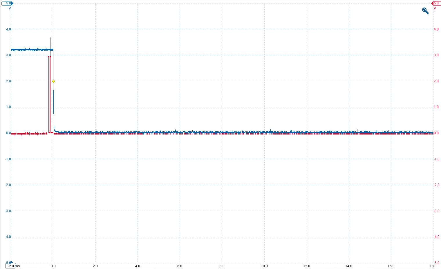
这显示了处理器复位线(蓝色)和从处理器到 SBC(红色)的 SPI 数据 SDO,这是处理器首次发送命令进入睡眠模式。
从 LIN 唤醒后,会发生以下情况:-
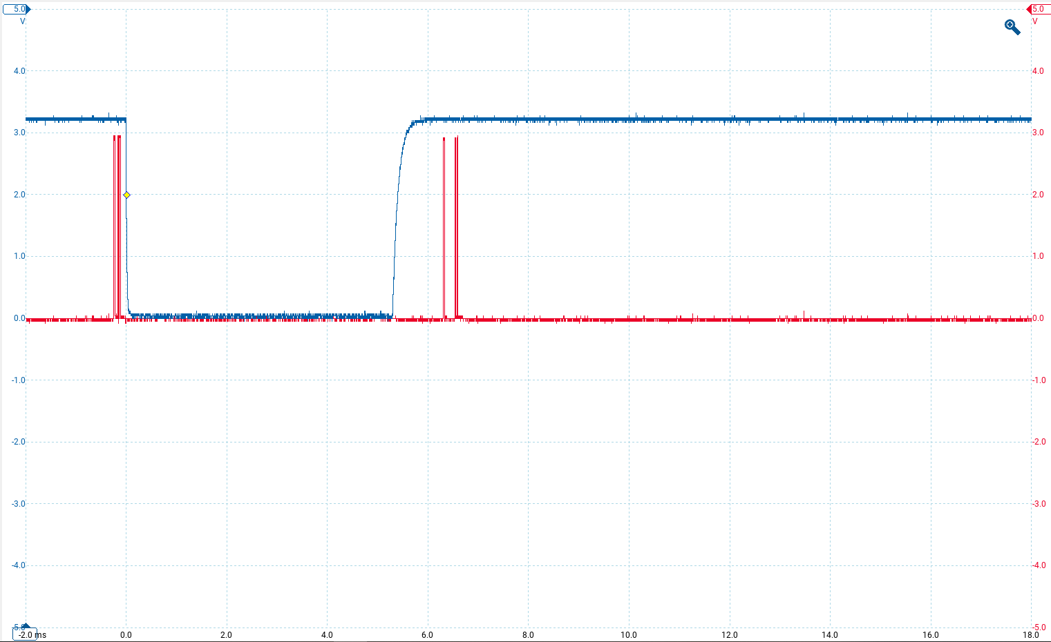
复位前的数据与之前相同,是关闭命令。重置后的数据是 SBC 的设置。
有谁知道为什么SBC芯片是这样的?
// DSPIC33CH128MP506 Configura
tion Bit Settings
// ‘C’ source line config statements
// FSEC
#pragma config BWRP = OFF // Boot Segment Write-Protect bit (Boot Segment may be written)
#pragma config BSS = DISABLED // Boot Segment Code-Protect Level bits (No Protection (other than BWRP))
#pragma config BSEN = OFF // Boot Segment Control bit (No Boot Segment)
#pragma config GWRP = OFF // General Segment Write-Protect bit (General Segment may be written)
#pragma config GSS = DISABLED // General Segment Code-Protect Level bits (No Protection (other than GWRP))
#pragma config CWRP = OFF // Configuration Segment Write-Protect bit (Configuration Segment may be written)
#pragma config CSS = DISABLED // Configuration Segment Code-Protect Level bits (No Protection (other than CWRP))
#pragma config AIVTDIS = OFF // Alternate Interrupt Vector Table bit (Disabled AIVT)
// FBSLIM
#pragma config BSLIM = 0x1FFF // Boot Segment Flash Page Address Limit bits (Enter Hexadecimal value)
// FSIGN
// FOSCSEL
#pragma config FNOSC = PRI // PRIPLL // Oscillator Source Selection (Primary Oscillator with PLL module (XT + PLL, HS + PLL, EC + PLL))
#pragma config IESO = OFF // Two-speed Oscillator Start-up Enable bit (Start up with user-selected oscillator source)
// FOSC
#pragma config POSCMD = EC // Primary Oscillator Mode Select bits (EC (External Clock) Mode)
#pragma config OSCIOFNC = OFF // OSC2 Pin Function bit (OSC2 is clock output)
#pragma config FCKSM = CSDCMD // Clock Switching Mode bits (Both Clock switching and Fail-safe Clock Monitor are disabled)
#pragma config XTCFG = G0 // XT Config (4-8 MHz crystals)
#pragma config XTBST = DISABLE // XT Boost (Default kick-start)
// FWDT
#pragma config RWDTPS = PS16384 // Run Mode Watchdog Timer Post Scaler select bits (1:16384)
#pragma config RCLKSEL = LPRC // Watchdog Timer Clock Select bits (Always use LPRC)
#pragma config WINDIS = ON // Watchdog Timer Window Enable bit (Watchdog Timer operates in Non-Window mode)
#pragma config WDTWIN = WIN25 // Watchdog Timer Window Select bits (WDT Window is 25% of WDT period)
#pragma config SWDTPS = PS1048576 // Sleep Mode Watchdog Timer Post Scaler select bits (1:1048576)
#pragma config FWDTEN = ON_SW // Watchdog Timer Enable bit (WDT controlled via SW, use WDTCON.ON bit)
// FICD
#pragma config ICS = PGD1 // ICD Communication Channel Select bits (Communicate on PGC1 and PGD1)
#pragma config JTAGEN = OFF // JTAG Enable bit (JTAG is disabled)
// FDMTIVTL
#pragma config DMTIVTL = 0xFFFF // Dead Man Timer Interval low word (Enter Hexadecimal value)
// FDMTIVTH
#pragma config DMTIVTH = 0xFFFF // Dead Man Timer Interval high word (Enter Hexadecimal value)
// FDMTCNTL
#pragma config DMTCNTL = 0xFFFF // Lower 16 bits of 32 bit DMT instruction count time-out value (0-0xFFFF) (Enter Hexadecimal value)
// FDMTCNTH
#pragma config DMTCNTH = 0xFFFF // Upper 16 bits of 32 bit DMT instruction count time-out value (0-0xFFFF) (Enter Hexadecimal value)
// FDMT
#pragma config DMTDIS = OFF // Dead Man Timer Disable bit (Dead Man Timer is Disabled and can be enabled by software)
// FDEVOPT
#pragma config ALTI2C1 = OFF // Alternate I2C1 Pin bit (I2C1 mapped to SDA1/SCL1 pins)
#pragma config ALTI2C2 = OFF // Alternate I2C2 Pin bit (I2C2 mapped to SDA2/SCL2 pins)
#pragma config SMBEN = SMBUS // SM Bus Enable (SMBus input threshold is enabled)
#pragma config SPI2PIN = PPS // SPI2 Pin Select bit (SPI2 uses I/O remap (PPS) pins)
// FALTREG
#pragma config CTXT1 = OFF // Specifies Interrupt Priority Level (IPL) Associated to Alternate Working Register 1 bits (Not Assigned)
#pragma config CTXT2 = OFF // Specifies Interrupt Priority Level (IPL) Associated to Alternate Working Register 2 bits (Not Assigned)
#pragma config CTXT3 = OFF // Specifies Interrupt Priority Level (IPL) Associated to Alternate Working Register 3 bits (Not Assigned)
#pragma config CTXT4 = OFF // Specifies Interrupt Priority Level (IPL) Associated to Alternate Working Register 4 bits (Not Assigned)
// FMBXM
#pragma config MBXM0 = S2M // Mailbox 0 data direction (Mailbox register configured for Main data read (Secondary to Main data transfer))
#pragma config MBXM1 = S2M // Mailbox 1 data direction (Mailbox register configured for Main data read (Secondary to Main data transfer))
#pragma config MBXM2 = S2M // Mailbox 2 data direction (Mailbox register configured for Main data read (Secondary to Main data transfer))
#pragma config MBXM3 = S2M // Mailbox 3 data direction (Mailbox register configured for Main data read (Secondary to Main data transfer))
#pragma config MBXM4 = S2M // Mailbox 4 data direction (Mailbox register configured for Main data read (Secondary to Main data transfer))
#pragma config MBXM5 = S2M // Mailbox 5 data direction (Mailbox register configured for Main data read (Secondary to Main data transfer))
#pragma config MBXM6 = S2M // Mailbox 6 data direction (Mailbox register configured for Main data read (Secondary to Main data transfer))
#pragma config MBXM7 = S2M // Mailbox 7 data direction (Mailbox register configured for Main data read (Secondary to Main data transfer))
#pragma config MBXM8 = S2M // Mailbox 8 data direction (Mailbox register configured for Main data read (Secondary to Main data transfer))
#pragma config MBXM9 = S2M // Mailbox 9 data direction (Mailbox register configured for Main data read (Secondary to Main data transfer))
#pragma config MBXM10 = S2M // Mailbox 10 data direction (Mailbox register configured for Main data read (Secondary to Main data transfer))
#pragma config MBXM11 = S2M // Mailbox 11 data direction (Mailbox register configured for Main data read (Secondary to Main data transfer))
#pragma config MBXM12 = S2M // Mailbox 12 data direction (Mailbox register configured for Main data read (Secondary to Main data transfer))
#pragma config MBXM13 = S2M // Mailbox 13 data direction (Mailbox register configured for Main data read (Secondary to Main data transfer))
#pragma config MBXM14 = S2M // Mailbox 14 data direction (Mailbox register configured for Main data read (Secondary to Main data transfer))
#pragma config MBXM15 = S2M // Mailbox 15 data direction (Mailbox register configured for Main data read (Secondary to Main data transfer))
// FMBXHS1
#pragma config MBXHSA = MBX15 // Mailbox handshake protocol block A register assignment (MSIxMBXD15 assigned to mailbox handshake protocol block A)
#pragma config MBXHSB = MBX15 // Mailbox handshake protocol block B register assignment (MSIxMBXD15 assigned to mailbox handshake protocol block B)
#pragma config MBXHSC = MBX15 // Mailbox handshake protocol block C register assignment (MSIxMBXD15 assigned to mailbox handshake protocol block C)
#pragma config MBXHSD = MBX15 // Mailbox handshake protocol block D register assignment (MSIxMBXD15 assigned to mailbox handshake protocol block D)
// FMBXHS2
#pragma config MBXHSE = MBX15 // Mailbox handshake protocol block E register assignment (MSIxMBXD15 assigned to mailbox handshake protocol block E)
#pragma config MBXHSF = MBX15 // Mailbox handshake protocol block F register assignment (MSIxMBXD15 assigned to mailbox handshake protocol block F)
#pragma config MBXHSG = MBX15 // Mailbox handshake protocol block G register assignment (MSIxMBXD15 assigned to mailbox handshake protocol block G)
#pragma config MBXHSH = MBX15 // Mailbox handshake protocol block H register assignment (MSIxMBXD15 assigned to mailbox handshake protocol block H)
// FMBXHSEN
#pragma config HSAEN = OFF // Mailbox A data flow control protocol block enable (Mailbox data flow control handshake protocol block disabled.)
#pragma config HSBEN = OFF // Mailbox B data flow control protocol block enable (Mailbox data flow control handshake protocol block disabled.)
#pragma config HSCEN = OFF // Mailbox C data flow control protocol block enable (Mailbox data flow control handshake protocol block disabled.)
#pragma config HSDEN = OFF // Mailbox D data flow control protocol block enable (Mailbox data flow control handshake protocol block disabled.)
#pragma config HSEEN = OFF // Mailbox E data flow control protocol block enable (Mailbox data flow control handshake protocol block disabled.)
#pragma config HSFEN = OFF // Mailbox F data flow control protocol block enable (Mailbox data flow control handshake protocol block disabled.)
#pragma config HSGEN = OFF // Mailbox G data flow control protocol block enable (Mailbox data flow control handshake protocol block disabled.)
#pragma config HSHEN = OFF // Mailbox H data flow control protocol block enable (Mailbox data flow control handshake protocol block disabled.)
// FCFGPRA0
#pragma config CPRA0 = MAIN // Pin RA0 Ownership Bits (Main core owns pin.)
#pragma config CPRA1 = MAIN // Pin RA1 Ownership Bits (Main core owns pin.)
#pragma config CPRA2 = MAIN // Pin RA2 Ownership Bits (Main core owns pin.)
#pragma config CPRA3 = MAIN // Pin RA3 Ownership Bits (Main core owns pin.)
#pragma config CPRA4 = MAIN // Pin RA4 Ownership Bits (Main core owns pin.)
// FCFGPRB0
#pragma config CPRB0 = MAIN // Pin RB0 Ownership Bits (Main core owns pin.)
#pragma config CPRB1 = MAIN // Pin RB1 Ownership Bits (Main core owns pin.)
#pragma config CPRB2 = MAIN // Pin RB2 Ownership Bits (Main core owns pin.)
#pragma config CPRB3 = MAIN // Pin RB3 Ownership Bits (Main core owns pin.)
#pragma config CPRB4 = MAIN // Pin RB4 Ownership Bits (Main core owns pin.)
#pragma config CPRB5 = MAIN // Pin RB5 Ownership Bits (Main core owns pin.)
#pragma config CPRB6 = MAIN // Pin RB6 Ownership Bits (Main core owns pin.)
#pragma config CPRB7 = MAIN // Pin RB7 Ownership Bits (Main core owns pin.)
#pragma config CPRB8 = MAIN // Pin RB8 Ownership Bits (Main core owns pin.)
#pragma config CPRB9 = MAIN // Pin RB9 Ownership Bits (Main core owns pin.)
#pragma config CPRB10 = MAIN // Pin RB10 Ownership Bits (Main core owns pin.)
#pragma config CPRB11 = MAIN // Pin RB11 Ownership Bits (Main core owns pin.)
#pragma config CPRB12 = MAIN // Pin RB12 Ownership Bits (Main core owns pin.)
#pragma config CPRB13 = MAIN // Pin RB13 Ownership Bits (Main core owns pin.)
#pragma config CPRB14 = MAIN // Pin RB14 Ownership Bits (Main core owns pin.)
#pragma config CPRB15 = MAIN // Pin RB15 Ownership Bits (Main core owns pin.)
// FCFGPRC0
#pragma config CPRC0 = MAIN // Pin RC0 Ownership Bits (Main core owns pin.)
#pragma config CPRC1 = MAIN // Pin RC1 Ownership Bits (Main core owns pin.)
#pragma config CPRC2 = MAIN // Pin RC2 Ownership Bits (Main core owns pin.)
#pragma config CPRC3 = MAIN // Pin RC3 Ownership Bits (Main core owns pin.)
#pragma config CPRC4 = MAIN // Pin RC4 Ownership Bits (Main core owns pin.)
#pragma config CPRC5 = MAIN // Pin RC5 Ownership Bits (Main core owns pin.)
#pragma config CPRC6 = MAIN // Pin RC6 Ownership Bits (Main core owns pin.)
#pragma config CPRC7 = MAIN // Pin RC7 Ownership Bits (Main core owns pin.)
#pragma config CPRC8 = MAIN // Pin RC8 Ownership Bits (Main core owns pin.)
#pragma config CPRC9 = MAIN // Pin RC9 Ownership Bits (Main core owns pin.)
#pragma config CPRC10 = MAIN // Pin RC10 Ownership Bits (Main core owns pin.)
#pragma config CPRC11 = MAIN // Pin RC11 Ownership Bits (Main core owns pin.)
#pragma config CPRC12 = MAIN // Pin RC12 Ownership Bits (Main core owns pin.)
#pragma config CPRC13 = MAIN // Pin RC13 Ownership Bits (Main core owns pin.)
#pragma config CPRC14 = MAIN // Pin RC14 Ownership Bits (Main core owns pin.)
#pragma config CPRC15 = MAIN // Pin RC15 Ownership Bits (Main core owns pin.)
// FCFGPRD0
#pragma config CPRD0 = MAIN // Pin RD0 Ownership Bits (Main core owns pin.)
#pragma config CPRD1 = MAIN // Pin RD1 Ownership Bits (Main core owns pin.)
#pragma config CPRD2 = MAIN // Pin RD2 Ownership Bits (Main core owns pin.)
#pragma config CPRD3 = MAIN // Pin RD3 Ownership Bits (Main core owns pin.)
#pragma config CPRD4 = MAIN // Pin RD4 Ownership Bits (Main core owns pin.)
#pragma config CPRD5 = MAIN // Pin RD5 Ownership Bits (Main core owns pin.)
#pragma config CPRD6 = MAIN // Pin RD6 Ownership Bits (Main core owns pin.)
#pragma config CPRD7 = MAIN // Pin RD7 Ownership Bits (Main core owns pin.)
#pragma config CPRD8 = MAIN // Pin RD8 Ownership Bits (Main core owns pin.)
#pragma config CPRD9 = MAIN // Pin RD9 Ownership Bits (Main core owns pin.)
#pragma config CPRD10 = MAIN // Pin RD10 Ownership Bits (Main core owns pin.)
#pragma config CPRD11 = MAIN // Pin RD11 Ownership Bits (Main core owns pin.)
#pragma config CPRD12 = MAIN // Pin RD12 Ownership Bits (Main core owns pin.)
#pragma config CPRD13 = MAIN // Pin RD13 Ownership Bits (Main core owns pin.)
#pragma config CPRD14 = MAIN // Pin RD14 Ownership Bits (Main core owns pin.)
#pragma config CPRD15 = MAIN // Pin RD15 Ownership Bits (Main core owns pin.)
// FCFGPRE0
#pragma config CPRE0 = MAIN // Pin RE0 Ownership Bits (Main core owns pin.)
#pragma config CPRE1 = MAIN // Pin RE1 Ownership Bits (Main core owns pin.)
#pragma config CPRE2 = MAIN // Pin RE2 Ownership Bits (Main core owns pin.)
#pragma config CPRE3 = MAIN // Pin RE3 Ownership Bits (Main core owns pin.)
#pragma config CPRE4 = MAIN // Pin RE4 Ownership Bits (Main core owns pin.)
#pragma config CPRE5 = MAIN // Pin RE5 Ownership Bits (Main core owns pin.)
#pragma config CPRE6 = MAIN // Pin RE6 Ownership Bits (Main core owns pin.)
#pragma config CPRE7 = MAIN // Pin RE7 Ownership Bits (Main core owns pin.)
#pragma config CPRE8 = MAIN // Pin RE8 Ownership Bits (Main core owns pin.)
#pragma config CPRE9 = MAIN // Pin RE9 Ownership Bits (Main core owns pin.)
#pragma config CPRE10 = MAIN // Pin RE10 Ownership Bits (Main core owns pin.)
#pragma config CPRE11 = MAIN // Pin RE11 Ownership Bits (Main core owns pin.)
#pragma config CPRE12 = MAIN // Pin RE12 Ownership Bits (Main core owns pin.)
#pragma config CPRE13 = MAIN // Pin RE13 Ownership Bits (Main core owns pin.)
#pragma config CPRE14 = MAIN // Pin RE14 Ownership Bits (Main core owns pin.)
#pragma config CPRE15 = MAIN // Pin RE15 Ownership Bits (Main core owns pin.)
// FS1OSCSEL
#pragma config S1FNOSC = FRCDIVN // Oscillator Source Selection (Internal Fast RC (FRC) Oscillator with postscaler)
#pragma config S1IESO = ON // Two-speed Oscillator Start-up Enable bit (Start up device with FRC, then switch to user-selected oscillator source)
// FS1OSC
#pragma config S1OSCIOFNC = OFF // Secondary OSC2 Pin Function bit (OSC2 is clock output)
#pragma config S1FCKSM = CSDCMD // Clock Switching Mode bits (Both Clock switching and Fail-safe Clock Monitor are disabled)
// FS1WDT
#pragma config S1RWDTPS = PS1048576 // Run Mode Watchdog Timer Post Scaler select bits (1:1048576)
#pragma config S1RCLKSEL = LPRC // Watchdog Timer Clock Select bits (Always use LPRC)
#pragma config S1WINDIS = ON // Watchdog Timer Window Enable bit (Watchdog Timer operates in Non-Window mode)
#pragma config S1WDTWIN = WIN25 // Watchdog Timer Window Select bits (WDT Window is 25% of WDT period)
#pragma config S1SWDTPS = PS1048576 // Sleep Mode Watchdog Timer Post Scaler select bits (1:1048576)
#pragma config S1FWDTEN = ON // Watchdog Timer Enable bit (WDT enabled in hardware)
// FS1ICD
#pragma config S1ICS = PGD1 // ICD Communication Channel Select bits (Communicate on PGC1 and PGD1)
#pragma config S1ISOLAT = ON // Isolate the Secondary core subsystem from the Main subsystem during Debug (The Secondary can operate (in debug mode) even if the SLVEN bit in the MSI is zero.)
#pragma config S1NOBTSWP = OFF // BOOTSWP Instruction Enable/Disable bit (BOOTSWP instruction is disabled)
// FS1DEVOPT
#pragma config S1ALTI2C1 = OFF // Alternate I2C1 Pin bit (I2C1 mapped to SDA1/SCL1 pins)
#pragma config S1SPI1PIN = PPS // S1 SPI1 Pin Select bit (Secondary SPI1 uses I/O remap (PPS) pins)
#pragma config S1SSRE = ON // Secondary Secondary Reset Enable (Secondary generated resets will reset the Secondary Enable Bit in the MSI module)
#pragma config S1MSRE = ON // Main Secondary Reset Enable (The Main software oriented RESET events (RESET Op-Code, Watchdog timeout, TRAP reset, illegalInstruction) will also cause the Secondary subsystem to reset.)
// FS1ALTREG
#pragma config S1CTXT1 = OFF // Specifies Interrupt Priority Level (IPL) Associated to Alternate Working Register 1 bits (Not Assigned)
#pragma config S1CTXT2 = OFF // Specifies Interrupt Priority Level (IPL) Associated to Alternate Working Register 2 bits (Not Assigned)
#pragma config S1CTXT3 = OFF // Specifies Interrupt Priority Level (IPL) Associated to Alternate Working Register 3 bits (Not Assigned)
#pragma config S1CTXT4 = OFF // Specifies Interrupt Priority Level (IPL) Associated to Alternate Working Register 4 bits (Not Assigned)
// #pragma config statements should precede project file includes.
// Use project enums instead of #define for ON and OFF.
#include 《xc.h》
#include “p33CH128MP506.h”
int main(void) {
WDTCONLbits.ON = 0;
TRISBbits.TRISB9 = 0;
// Select SPI peripheral pin select
RPOR5 = 7; // output RP42 - to be CSN
RPOR6 = 6 + (5 《《 8); // outputs RP44 = 6 (clock) and RP45 = 5 (data out)
RPINR20 = 43; // input SPI input = RP43
RPOR12 = (7 《《 8) ; // RC9 for debug
RPOR18 = (6 《《 8) ; // Rd5 for debug
RPOR3 = 5;
SPI1CON1L = 0b0000011000100000;
SPI1BRGL = 50 ; // 50 gives ~100 kBaud 。 I don‘t know what is right or wrong here.
SPI1BRGH = 00 ;
SPI1CON2L = 0b0; // don’t override the mode bits
SPI1CON1H = 0b0011000000011000;
SPI1STATLbits.SPIROV = 0; // not sure what this is for
SPI1CON1Lbits.SPIEN = 1; // enable SPI1
int a = 0;
int b = 0;
do {
a++;
} while ( a《500 );
SPI1BUFL = 0x2005; // This sends 0x2005 on the SPI bus. The command is to configure to wake up on either LIN
do {
a = 0;
do {
a++;
} while ( a《20000 );
LATBbits.LATB9 = 0;
a = 0;
do {
a++;
} while ( a《20000 );
LATBbits.LATB9 = 1;
b++;
if (b 《 30)
{
SPI1BUFL = 0x0350; // this should reset the NCV7471 watchdog
}
else
{
SPI1BUFL = 0x0650; // This should make it sleep
}
} while (1);
}


 举报
举报


