本文罗列了各种不同的设计疏忽,探讨了每种失误导致电路故障的原因,并给出了如何避免这些设计缺陷的建议。本文以FR-4电介质、厚度0.0625in的双层PCB为例,电路板底层接地。工作频率介于315MHz到915MHz之间的不同频段,Tx和Rx功率介于-120dBm至+13dBm之间。表1列出了一些可能出现的PCB布局问题、原因及其影响。
表1. 典型的PCB布局问题和影响
Problem
Cause
Effect
LNA/tank circuit arrangement (receiver)
Inductor orientation
RF feedthrough
Degeneration/π-network arrangement (transmitter)
Inductor orientation
RF feedthrough
Shared ground vias between legs of π network
Via parasitics
Feedthrough, RF leakage
Shared ground vias between receiver blocks
Via parasitics
Crosstalk, RF feedthrough, RF leakage
Long traces for decoupling capacitors
Higher-impedance connections
Reduced decoupling
Wide component placement
Increased parasitics, ground loops
Detuning, crosstalk, feedthrough
Colinear traces in the transmitter circuit
Filter bypassing, i.e., power amplifier (PA) directly to antenna
Harmonics radiation
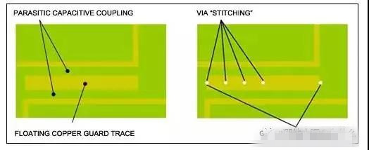
Top-layer copper pours
Parasitic coupling
RF leakage, RF interference
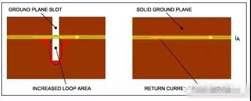
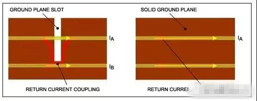
Discontinuous ground plane
Return current concentration
Crosstalk, feedthrough
Crystal connection trace length
Excess capacitance
LO frequency pulling
Crystal connection trace separation
Excess capacitance
LO frequency pulling
Ground plane under crystal pads
Excess capacitance
LO frequency pulling
Planar PCB trace inductors
Poor inductance control
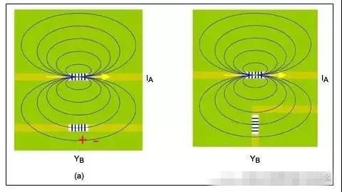
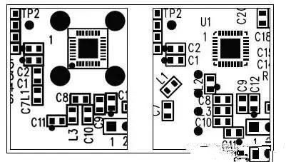
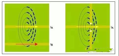
其中大多数问题源于少数几个常见原因,我们将对此逐一讨论。

 举报
举报


 举报
举报

 举报
举报
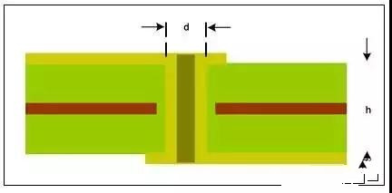


 举报
举报

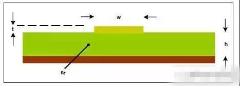



 举报
举报

