结束语
许多市场对输出电压高于或低于输入电压(升压/降压)的高效率同相转换器的需求都在不断增长。ADI 公司的双通道同步开关控制器ADP1877允许用低损耗MOSFET代替常用于功率级的高损耗功率二极管,从而提高效率,降低成本,缩小电路尺寸,使系统达到苛刻的能耗要求。只要遵循几项原则就能快速算出可靠补偿所需的元件值,并且利用常见的现成器件便可实现高效率。
参考电路
Barrow, Jeff. "Reducing Ground Bounce in DC-to-DC Converters—Some Grounding Essentials." Analog Dialogue. 41-2, pp. 2-7. 2007.
1Ćuk, Slobodan and R.D. Middlebrook. "Coupled-Inductor and Other Extensions of a New Optimum Topology Switching DC-DC Converter." Advances in Switched-Mode Power Conversion. Volumes I & II. Irvine, CA: TESLAco. 1983.
2Erickson, Robert and Dragan Maksimović. Fundamentals of Power Electronics. Chapter 12, Section 1. Norwell, MA: Kluwer Academic Publishers. 2001.
3Ridley, Raymond. "A New Small-Signal Model for Current-Mode Control." PhD Dissertation, Virginia Polytechnic Institute and State University. November 1990.
附录
ADP1877是一款Flex-ModeTM(ADI公司专有架构)双通道开关 控制器,如图A所示,其集成驱动器可驱动N沟道同步功率 MOSFET。两路PWM输出相移 180°,可降低输入均方根电流, 从而使所需的输入电容最小。
图 A. ADP1877 示意框图。仅显示通道 1;通道 2 与之完全相同,带后缀 2。ADP1877 内置升压二极管,因而整体元件数量和系统成本得以 减少。在小负载时,可以将它设置为高效率脉冲跳跃工作模式, 也可以是 PWM 连续传导工作模式。
ADP1877 内置外部可调软启动功能、输出过压保护、外部可调 电流限制、电源良好指示,并提供 200 kHz 至 1.5 MHz 的可编程 振荡器频率。工作温度范围为–40°C 至+85°C 时,输出电压精 度为±0.85%;工作温度范围为–40°C 至+125°C 结温范围时, 输出电压精度为±1.5%。其工作电源电压为 2.75 V 至 14.5 V, 采用 32 引脚、5 mm × 5 mm LFCSP 封装。
Matt Kessler
Matt Kessler is an applications engineer for Power Management Products in the Customer Applications Group in Fort Collins, CO. Responsible for technical support for a wide range of a products and customers, Matt is also one of the original architects and developers of ADIsimPower. Matt earned his BSEE from the University of Texas at Dallas and is currently pursuing his MSEE at Colorado State University. He has been with Analog Devices since 2007.
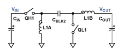
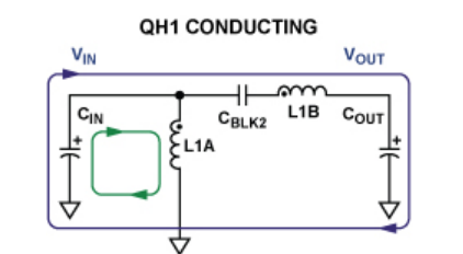
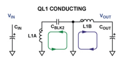
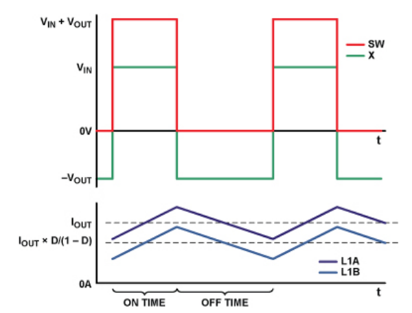
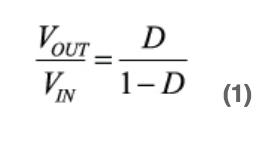 上式表明:如果占空比大于 0.5,输出端将获得较高的调节电压(升压);如果占空比小于 0.5,调节电压会较低(降压)。此外还可分析得到其它相关结果:在无损系统中,能量传输电容(CBLK2)上的稳态电压等于VOUT;流经输出电感(L1B)的直流电流值等于IOUT;流经地基准电感(L1A)的直流电流值等于IOUT ×VOUT/VIN。该能量传输电容还能提供VIN至VOUT的隔直。当存在输出短路风险时,此特性很有用。
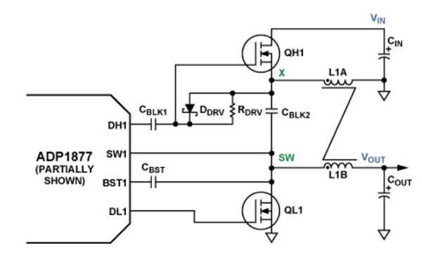
 匝数比最好为 1:1,因为对于给定水平的输出电压纹波,此时各绕组只需要分立电感所需电感的一半1。可以使用 1:1 以外的匝数比,但其结果将无法用本文中的方程式准确描述。
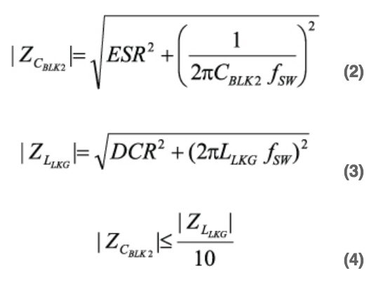
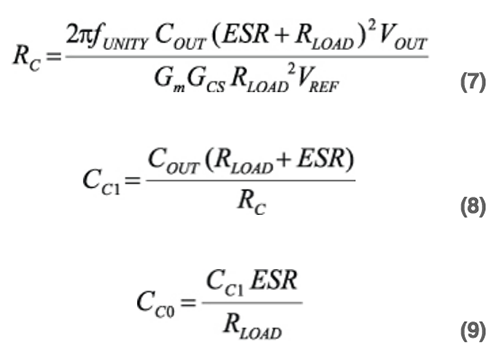
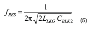 在此频率时,可能有 300°或更大的"高Q"相位迟滞。为了避免转换器在整个负载范围内相位裕量偏小的问题,目标交越频率(fUNITY)应为fRES的 1/10。此谐振的阻尼主要取决于输出负载电阻和耦合电感的直流电阻。在较小程度上,阻尼还取决于能量传输电容的等效串联电阻(ESR)和功率MOSFET(QHl和QL1)的导通电阻。因此,当输出负载电阻改变时,闭环传递函数的特征在该频率时发生明显变化也不足为奇。
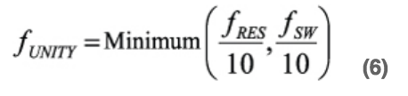 图6 显示同步反相SEPIC 降压/升压拓扑结构中ADP1877反馈环路的等效电路。上框包含功率级和电流环路,下框包含电压反馈环路和补偿电路。
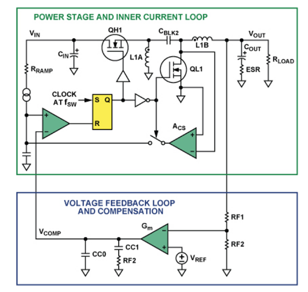
 转换器的跨导GCS利用下式计算:
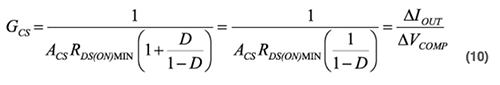 COUT是转换器的输出电容。ESR是该输出电容的等效串联电阻。RLOAD是最小输出负载电阻。ACS是电流检测增益,对于ADP1877,它可以在 3 V/V至 24 V/V范围内以离散步进选择。Gm是误差放大器的跨导,ADP1877 为 550 μs。VREF是与误差放大器的正输入端相连的基准电压,ADP1877 为 0.6 V。
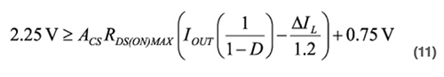 其中∆IL为峰峰值电感纹波电流。
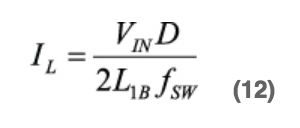 如果斜率补偿过多,此处的方程式精确度将会下降:直流增益将降低,输出滤波器将引起主极点的频率位置提高。
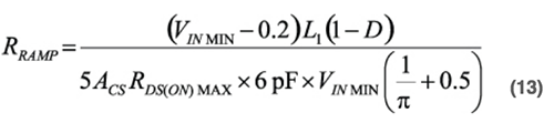 值得注意的是,随着增强后的次级开关电阻RDS(ON)降低,采样极点的Q也会下降。如果这一因素与其它相关容差一起导致Q小于0.25,则应进行仿真,确保在考虑容差的情况下,转换器不会有过多斜率补偿,并且不是太偏向于电压模式。RRAMP的值必须使得ADP1877 RAMP引脚的电流在 6 μA至 200 μA范围内,其计算公式 14 如下:
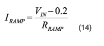 功率器件应力
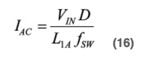 知道这些值后,可以很快算出流经各开关的电流均方根值。这些值与所选MOSFET的RDS(ON)MAX共同确保MOSFET具有热稳定性,同时功耗足够低,以满足效率要求。
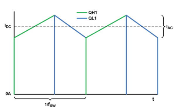
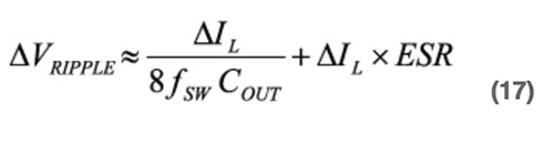 流经输出电容的电流均方根值(I rms COUT)为:
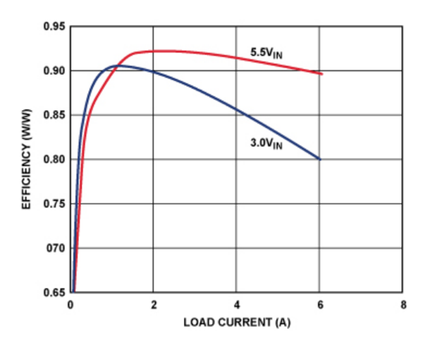 方程式 12 所表示的峰峰值电感电流(∆IL)取决于输入电压,因此必须确保当此参数改变时,输出电压纹波不会超过规定值,并且流经输出电容的均方根电流不会超过其额定值。
 结束语
结束语

