为了降低Iq或者不低Iq,这就是问题......对于许多汽车系统而言,无疑使用莎士比亚,扭曲为工程主题,除此之外,静态电流(Iq)是一个大问题。
低多低?
如何实现它?
有什么权衡取舍?
故事通常是由汽车自有设备制造商(OEM)设定的整体系统Iq目标开始,然后将其划分为关键系统块;
通常,剩余部分是
电源需要遵守的。
次级负载点(POL)稳压器通常可以禁用,每个功耗仅为1μA。
然而,来自电池的主电源通常是静态电流的主要消耗者。
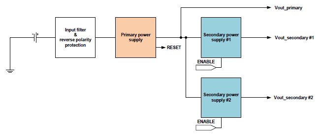
图1 - 典型的汽车系统电源框图
在负载电流高或需要最小化功耗的情况下,需要考虑开关模式电源(SMPS)。
正如我之前的博客中所讨论的,实现这一目标的一种方法是使用脉冲频率调制(PFM)或突发模式等技术,但另一种方法可能是使用集成混合拓扑,其中线性稳压器和SMPS是
并行使用。
当系统处于唤醒状态时,SMPS被启用且线性稳压器被禁用,当系统处于静止状态时,SMPS被禁用并启用线性稳压器。
线性稳压器吸收低Iq。
这种方法可以提供低至25μA(典型值)的Iq。
开关功能(SMPS和线性模式之间)可通过监控负载电流实现自动化,例如使用安森美
半导体NCV891330低Iq双模式降压稳压器,或手动系统控制开关,例如
NCV97310多输出电源管理单元。
两种情况下的输出电容都可以在模式之间提供平滑切换,而不会出现毛刺。
然而,这种方法的一个限制是输入电压顺应性。
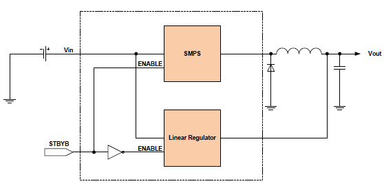
图2 - 混合线性/ SMPS转换器
如果SMPS具有PMOS高侧开关,则不需要自举,并且可以实现100%的占空比,然后只考虑PMOS本身的电压降(输入滤波器除外)。
如果SMPS有一个NMOS高侧开关,那么将有一个最大占空比,设置为允许NMOS引导带每个周期补充一次。
该最大占空比限制了最小输入电压。
例如,具有5.0 V输出和0.5 A负载的NCV891330能够输入低至5.34 V的电压。任何低于此的输入电压都需要预增压器,电池和主电源之间的升压控制器,例如
NCV8877启动停止非同步升压控制器。例如,NCV8877在非激活时将为Iq总数再增加12μA(典型值)。
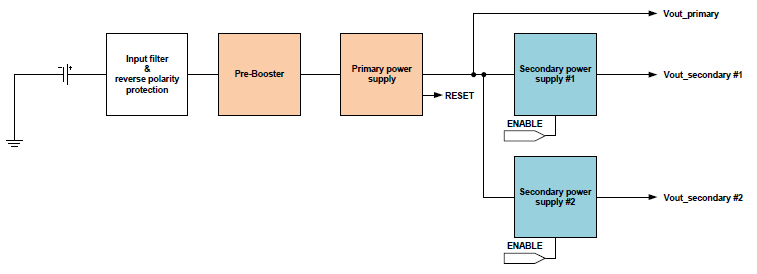
图3 - 具有预增压器的典型汽车系统电源框图
如果负载电流较低或效率较低,则可以考虑线性稳压器。
采用这种方法,使用MOS线性稳压器可以实现低至21μA(典型值)的静态电流。
双极线性稳压器将消耗更多的Iq,但与MOS线性稳压器相比,这通常可以与较低的成本和固有的反极性保护(PNP)进行折衷。
虽然可以实现较低的Iq电平,但必须考虑最小特征集,例如复位或看门狗
电路。
如果发生某些电源故障导致MCU“锁定”,则为关键模块供电的主电源(如微控制器或CAN需要)应能够重置微控制器(MCU)。
线性稳压器的输入电压兼容性由其高侧开关的电压降确定。
通常,这可低至200 mV。
线性稳压器的一个重要方面是,当输入到输出电压差低于高侧开关的电压降时,输出电压将随输入电压下降而降低输出电压。
如果负载(通常是MCU)接受低容差输入电源,则线性稳压器输出仍将处于活动状态,从而允许MCU有更多时间检查其输入,保留存储器设置以及有序关闭。
那么,是或不是?
如果系统可以关闭,那么,不要 - 低Iq调节器不是这种系统的必要功能。
如果系统无法关闭,那么 - 低 - Iq调节器是必要的功能。
无论是线性,混合线性SMPS还是完整SMPS,哪种方法取决于系统级要求以及可以或不可以进行的权衡。
以上来自于谷歌翻译
以下为原文
To be low Iq or not to be low Iq, that is the ques
tion… Doubtful use of Shakespeare, twisted to title an engineering topic, aside, quiescent current (Iq) is a big question for many automotive systems. How low is low? How does one achieve it? And what are the trade-offs? Very often the story starts with an overall system Iq target set by the automotive Own Equipment Manufacturer (OEM), which is then divided amongst the key system blocks; generally the remainder is what the power supply is required to comply with. The secondary, point-of-load (POL), regulators can often be disabled to consume as little as 1 µA each. However, the primary power supply, which sources from the battery, is often a major consumer of quiescent current.

Fig. 1 – Typical Automotive System Power Supply Block Diagram
Where the load current is high or power dissipation needs to be minimised then a switched mode power supply (SMPS) needs to be considered. As discussed in my previous blog, one way of achieving this is by use of techniques such as pulse frequency modulation (PFM) or burst-mode, but another means might be the use of an integrated hybrid topology where a linear regulator and an SMPS are used in parallel.
When the system is awake then the SMPS is enabled and the linear regulator disabled, and when the system is in its quiescent state then the SMPS is disabled and the linear regulator enabled. The linear regulator draws a low Iq. Such an approach can deliver an Iq as low as 25 µA (typ). The switching function (between SMPS and linear modes) can be automated by monitoring the load current, such as with the ON Semiconductor NCV891330 low-Iq dual-mode step-down regulator, or manual where the system controls the switching, such as with the NCV97310 multi-output power management unit. The output capacitance in both cases is relied upon to deliver smooth switching between modes, without glitches. One limitation of such approaches though is input voltage compliance.

Fig. 2 – Hybrid Linear/SMPS Converter
If the SMPS has a PMOS high-side switch, a boot-strap is not required and 100 % duty cycle is possible, then there is just the voltage drop across the PMOS itself to be considered (input filter aside). If the SMPS has an NMOS high-side switch then there will be a maximum duty cycle, set to allow the NMOS boot-strap to replenish itself per cycle. This maximum duty cycle limits the minimum input voltage. For example the NCV891330 with a 5.0 V output and 0.5 A load is capable of input voltages as low as 5.34 V. Any input voltage lower than this requires a pre-booster, a boost controller between the battery and the primary power supply, such as the NCV8877 start stop non-synchronous boost controller.The NCV8877, for example, will add a further 12 µA (typ) to the Iq total when inactive.

Fig. 3 - Typical Automotive System Power Supply Block Diagram with Pre-Booster
If the load current is low or efficiency is a lessor concern then a linear regulator can be considered. With this approach then quiescent currents as low as 21 µA (typ) can be achieved, using a MOS linear regulator. A bipolar linear regulator will consume more Iq but this can be typically traded-off against a lower cost and intrinsic reverse polarity protection (PNP), as compared to the MOS linear regulator.
While lower Iq levels are possible to achieve, a minimum feature set has to be considered such as a reset or watchdog circuit. The primary power supply powering the key blocks, such as the micro-controller or CAN needs, should be able to reset the micro-controller (MCU) if some power supply glitch occurs that causes the MCU to ‘lock-up’.
The input voltage compliance of the linear regulator is determined by the voltage drop-out of its high side switch. Typically this can be as low as 200 mV. An important facet of the linear regulator is that as the input to output voltage differential falls below the voltage drop-out of the high-side switch, the output voltage will follow the input voltage as it falls minus the drop-out voltage. If the load, typically an MCU, accepts a low tolerance input supply then the linear regulator output will still be active, allowing the MCU more time to check its inputs, retain memory settings, and shut-down in an orderly manner.
So, to be or not to be? If the system can be switched off then, not to be – low Iq regulators are not a necessary feature of such a system. If the system can’t be switched off then, to be – low Iq regulators are a necessary feature. Which approach, whether linear, hybrid linear-SMPS or full SMPS depends upon the system level requirements and the trade-offs that can or cannot be made.

